High-Performance 4-Layer Hybrid PCBs with RO4350B and S1000-2M for Advanced RF Applications
(Custom PCBs are tailored products; the images and specifications provided are for reference only.)
Introduction of RO4350B
Rogers RO4350B materials are proprietary woven glass reinforced hydrocarbon/ceramics that offer electrical performance comparable to PTFE/woven glass while maintaining the manufacturability of epoxy/glass. These laminates ensure tight control over the dielectric constant (Dk) and exhibit low loss, using standard epoxy/glass processing methods.
RO4350B laminates are significantly more cost-effective than conventional microwave laminates and do not require special through-hole treatments or handling procedures that PTFE-based materials do. Rated UL 94 V-0, they are suitable for active devices and high-power RF designs. The thermal coefficient of expansion (CTE) of RO4350B closely matches that of copper, ensuring excellent dimensional stability, crucial for mixed dielectric multilayer constructions. With a Tg of over 280°C (536°F), RO4350B maintains stable expansion characteristics throughout the circuit processing temperature range.
Features of RO4350B
Dielectric Constant: DK 3.48 ± 0.05 at 10GHz/23°C
Dissipation Factor: 0.0037 at 10GHz/23°C
Thermal Conductivity: 0.69 W/m/°K
X-axis CTE: 10 ppm/°C, Y-axis CTE: 12 ppm/°C, Z-axis CTE: 32 ppm/°C
High Tg Value: >280°C
Low Water Absorption: 0.06%
Features of S1000-2M:
Lower Z-axis CTE for improved through-hole reliability
Excellent mechanical processability and thermal resistance
Lead-free compatible
Tg of 180°C (DSC), UV blocking/AOI compatible
High heat resistance
Excellent anti-CAF performance
Low water absorption
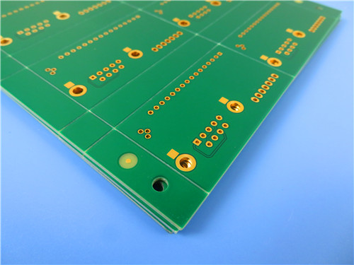
Basic PCB Specifications
| Specification | Details |
|---|---|
| Base Material | RO4350B and S1000-2M (FR-4) mixed |
| Layer Count | 4 layers |
| Board Dimensions | 105mm x 95mm (8 PCS), ± 0.15mm |
| Minimum Trace/Space | 5/4 mils |
| Minimum Hole Size | 0.35mm |
| Blind Vias | Top layer to second layer, third layer to bottom layer |
| Finished Board Thickness | 1.6mm |
| Finished Copper Weight | 1oz (1.4 mils) inner/outer layers |
| Via Plating Thickness | 20 µm |
| Surface Finish | Electroless Nickel Immersion Gold (ENIG) |
| Top Silkscreen | White |
| Bottom Silkscreen | No |
| Top Solder Mask | Green |
| Bottom Solder Mask | No |
| Impedance Control | 50 ohm on 5mil / 9mil traces/gaps, top layer |
| Edge Plating | Designated area |
| Via Filling | 0.35mm vias filled and capped |
| Electrical Testing | 100% electrical test prior to shipment |
PCB Stack-Up (4-Layer Rigid PCB)
| Layer | Material | Thickness |
|---|---|---|
| Copper Layer 1 | Copper | 35 µm |
| Copper Layer 2 | RO4350B | 0.254 mm (10 mil) |
| Copper Layer 3 | Copper | 35 µm |
| Prepreg | 1080 RC63% | 0.0644 mm (2.5 mil) |
| Copper Layer 4 | Copper | 35 µm |
| S1000-2M | Core | 1.1 mm (43 mil) |
| Copper Layer 5 | Copper | 35 µm |
PCB Statistics:
Components: 33
Total Pads: 242
Through Hole Pads: 125
Top SMT Pads: 117
Bottom SMT Pads: 0
Vias: 49
Nets: 3
Artwork and Standards Information
Type of Artwork Supplied: Gerber RS-274-X
Accepted Standard: IPC-Class-2
Availability: Worldwide
Typical Applications
Commercial airline broadband antennas
Microstrip and stripline circuits
Millimeter wave applications
Radar systems
Guidance systems
Point-to-point digital radio antennas
